Research Paper Review: TPU
This paper assesses the effectiveness of a custom ASIC called a Tensor Processing Unit (TPU), which has been utilized in datacenters since 2015 to expedite the inference phase of neural networks (NN). The TPU features a 65,536 8-bit MAC matrix multiply unit that provides a peak throughput of 92 TeraOps/second (TOPS) and incorporates a large (28 MiB) software-managed on-chip memory. Unlike CPUs and GPUs, which employ time-varying optimizations to enhance average throughput, the TPU’s deterministic execution model better aligns with the 99th-percentile response-time requirement of NN applications, prioritizing guaranteed latency over fluctuating performance. The TPU boasts a compact size and low power consumption. On average, it outperforms contemporary GPUs or CPUs by approximately 15\(\times\) to 30\(\times\), with a TOPS/Watt ratio around 30\(\times\) to 80\(\times\) higher. Additionally, integrating the GPU’s GDDR5 memory into the TPU would triple the achieved TOPS and elevate the TOPS/Watt ratio to nearly 70\(\times\) that of the GPU and 200\(\times\) that of the CPU.
Paper Summary
Neural Networks
Neural networks consist of two main phases: training and inference, corresponding to development and production stages. Training, primarily done in floating point, has been popularized by GPUs due to their efficiency. However, for inference, quantization converts floating-point numbers to narrower integers, typically 8 bits, which are often sufficient. This approach significantly reduces energy consumption and chip area compared to floating-point operations. Popular NN architectures include MLP, CNN, and RNN, each requiring millions to hundreds of millions of weights, which can be time and energy-intensive to access. To optimize performance, weights are reused across batches of independent examples during inference or training.
This paper evaluates the TPU and compares its inference performance and power efficiency with contemporary CPUs and GPUs. Key findings from the study include the following: inference applications prioritize response time over throughput due to their user-facing nature; despite the K80 GPU’s higher peak performance and memory bandwidth, it is only slightly faster than the Haswell CPU for inference, primarily due to latency limitations; the TPU significantly outperforms both the K80 GPU and the Haswell CPU in inference speed, ranging from 15\(\times\) to 30\(\times\) faster; if the TPU had the same memory capacity as the K80 GPU, its performance would be boosted to be 30\(\times\) to 50\(\times\) faster than both the GPU and CPU; despite its smaller size and lower power consumption, the TPU provides significantly more MAC units and on-chip memory compared to the K80 GPU; finally, the performance per watt of the TPU exceeds contemporary CPUs and GPUs by 30\(\times\) to 80\(\times\), and with K80 memory, this margin could potentially increase to 70\(\times\) to 200\(\times\).
TPU
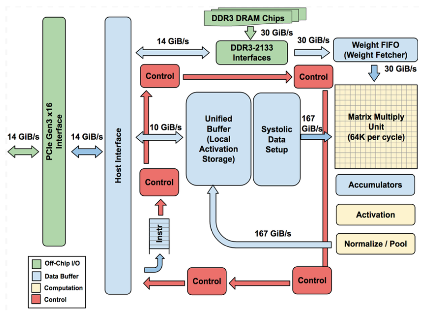
The objective was to enhance cost-performance by 10 times compared to GPUs. Within just 15 months, the TPU was conceptualized, validated, constructed, and implemented in data centers. Designed as a coprocessor for the PCIe I/O bus, akin to GPUs, it allows easy integration into existing servers. To streamline hardware design and debugging, the host server sends instructions to the TPU for execution rather than the TPU fetching them independently, resembling an FPU coprocessor more than a GPU. The aim was to execute entire inference models within the TPU, reducing reliance on the host CPU and ensuring flexibility to accommodate neural network demands from 2015 onwards. The TPU’s block diagram is illustrated in Figure 1, showcasing its internal architecture and connectivity. Key components include the Matrix Multiply Unit, housing 256x256 MAC units capable of 8-bit multiply-and-add operations. The Matrix Unit operates at varying speeds depending on the mix of weights and activations, supporting both dense matrices and convolutions. Sparse architectural support was omitted due to deployment timelines. Data flow involves staging weights through an on-chip FIFO from an off-chip DRAM called Weight Memory, while intermediate results are stored in the 24 MiB Unified Buffer. In the TPU’s die floor plan, the Unified Buffer occupies a significant portion and control constitutes only 2% of the design. TPU instructions adhere to the CISC tradition, featuring a repeat field, with an average of 10 to 20 clock cycles per instruction.
The TPU microarchitecture is designed to maximize the utilization of the matrix unit by employing a 4-stage pipeline for executing complex instructions, ensuring each instruction progresses through separate stages. To conserve energy, the matrix unit employs systolic execution, minimizing reads and writes to the Unified Buffer by combining data arriving from different directions at regular intervals. Compatibility with existing CPU and GPU software stacks was crucial for rapid adoption of the TPU. Typically, applications for the TPU are written in TensorFlow and compiled into an API that can also run on GPUs. Similar to GPUs, the TPU software stack consists of a User Space Driver and a Kernel Driver, with the latter managing memory and interrupts for long-term stability. The User Space Driver, which undergoes frequent changes, handles TPU execution, data formatting, API translation into TPU instructions, and application binary generation. Upon initial evaluation, the User Space Driver compiles a model, caching the program and writing weight images into the TPU’s memory, enabling subsequent evaluations to run at full speed.
Results
Performance: Rooflines, Response-Time, And Throughput
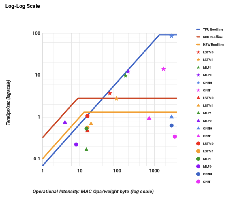
The researchers employ the Roofline Performance model, originally developed for high-performance computing (HPC), as a straightforward visual tool to identify performance bottlenecks. This model operates under the assumption that applications exceed on-chip cache capacities, leading to either computation or memory bandwidth limitations. In the context of HPC, the Y-axis signifies performance in floating-point operations per second, with the peak computation rate forming the “flat” part of the roofline. Meanwhile, the X-axis measures operational intensity, quantified as floating-point operations per byte of DRAM accessed. Figure 2 presents a log-log graph combining data. In this graph, stars represent the TPU, triangles denote the K80, and circles represent Haswell. Notably, all TPU stars lie at or above the rooflines of the other two platforms.
Cost-performance, TCO, and Performance/Watt
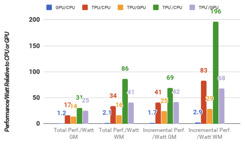
When procuring computers in bulk, the prioritization of cost-performance over raw performance becomes crucial. In the context of datacenter operations, the total cost of ownership (TCO) emerges as the most pertinent cost metric. While specific chip prices are subject to negotiation and cannot be disclosed due to business reasons, power consumption correlates with TCO. Hence, researchers employ performance per watt as a proxy for performance per TCO in this study. Figure 3 presents the geometric and weighted mean performance per watt for the K80 GPU and TPU relative to the Haswell CPU. Two distinct calculations of performance per watt are showcased: total and incremental. The total calculation encompasses the power consumed by the host CPU server when assessing performance per watt for the GPU and TPU, whereas the incremental calculation subtracts the host CPU server power beforehand. For total performance per watt, the K80 server outperforms the Haswell CPU by 1.2 to 2.1 times. In the scenario of incremental performance per watt, where Haswell server power is excluded, the K80 server surpasses the CPU by 1.7 to 2.9 times. The TPU server demonstrates significantly superior total performance per watt compared to the Haswell CPU, ranging from 17 to 34 times better, positioning it 14 to 16 times more efficient than the K80 server. The relative incremental performance per watt, which served as the impetus behind the development of a custom ASIC, indicates that the TPU outperforms the GPU by 41 to 83 times, resulting in 25 to 29 times greater performance per watt.
Energy Proportionality
Thermal Design Power (TDP) impacts the cost of power provisioning, as it necessitates supplying adequate power and cooling when hardware operates at full capacity. However, electricity costs are based on average consumption as workload fluctuates throughout the day. Research has advocated for energy proportionality, where servers should consume power in proportion to the workload they handle. Our power consumption estimates are based on the fraction of TDP observed in our datacenters.
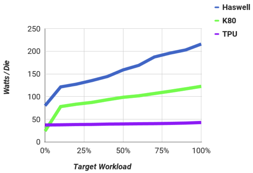
Performance and power measurements of servers, including CPUs, TPUs, and GPUs, were conducted as workload utilization varied from 0% to 100%, grouped in 10% increments. Figure 4 illustrates server power divided by the number of dies per server for the three chip types with varying workload for CNN0.
The TPU exhibits the lowest power consumption at 40W per die, but it lacks energy proportionality, using 88% of its full power at 10% workload due to a rushed design schedule without energy-saving features. Haswell demonstrates the best energy proportionality, using only 56% of its power at 10% workload compared to full load. The K80 GPU and LSTM1, which is not computation-bound, display similar energy proportionality trends.
Examining server power usage with accelerators hosting CNN0, when the GPU and TPU operate at full load, the CPU server consumes 52% of full power for the GPU and 69% for the TPU. Consequently, a Haswell server with four TPUs consumes less than 20% additional power while running CNN0 80 times faster than a Haswell server alone with two CPUs.
Evaluation of alternative TPU designs
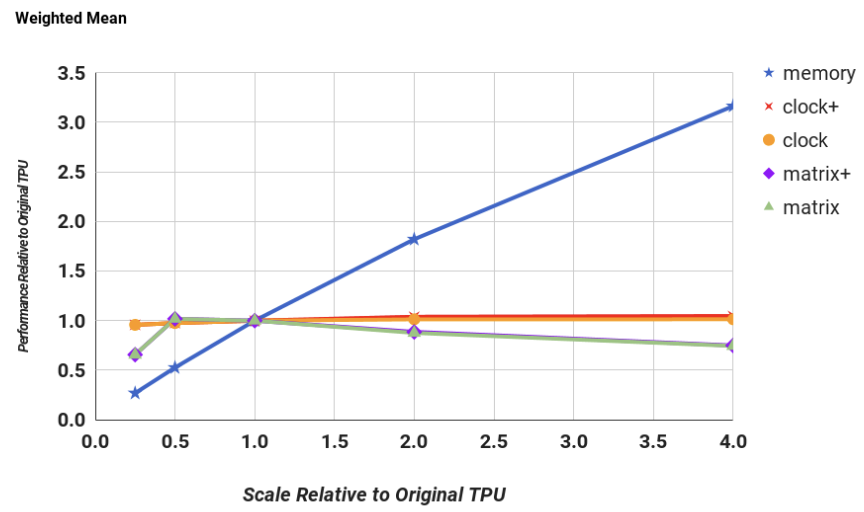
The TPU coprocessor, akin to an FPU, lends itself to relatively straightforward evaluation. A performance model was devised for six applications, with the differences between model results and hardware performance counters averaging below 10%. Performance was modeled as memory bandwidth, clock rate, number of accumulators, and matrix multiply unit size varied. Figure 5 depicts the mean performance sensitivity of the TPU die across these parameters, ranging from 0.25\(\times\) to 4\(\times\) scaling. Notably, increasing memory bandwidth has the most significant impact, with performance improving 3\(\times\) on average with a 4\(\times\) increase in memory. Clock rate has minimal benefit on average, particularly for memory-bound MLPs and LSTMs, while the impact on compute-bound CNNs is notable. Expanding the matrix unit size slightly degrades average performance due to internal fragmentation issues, particularly pronounced with larger matrices. Improvements in storage allocation have reduced memory requirements, allowing for marginally larger models. A hypothetical TPU die (TPU’) evaluation suggests that more aggressive logic synthesis and block design could increase clock rates by 50%, while integrating a GDDR5 memory interface could significantly enhance performance. However, these changes necessitate doubling the number of memory channels and slightly increasing die size. Overall, TPU’ exhibits substantial performance gains over Haswell and K80, particularly in total and incremental performance per watt metrics.
Critical Review
Pros
- The paper provides a thorough evaluation of the TPU across various parameters such as performance, power consumption, and energy proportionality
- The paper is well-organized and presents complex technical information in a clear and concise manner.
- The discussion addresses the main shortcomings of the paper.
Cons
- The paper does not include comparisons with other accelerators.
Takeaways
Despite residing on an I/O bus and having limited memory bandwidth, which constrains its utilization, the TPU demonstrates that even a small fraction of a large resource can yield significant performance benefits, as evidenced by the Roofline performance model. This suggests a ``Cornucopia Corollary” to Amdahl’s Law, where low utilization of a substantial, cost-effective resource can still deliver high performance. The TPU capitalizes on the significant reduction in energy and area afforded by 8-bit integer systolic matrix multipliers compared to the 32-bit floating-point datapaths of a K80 GPU. This allows for a considerable increase in MACs and on-chip memory, while consuming less power and occupying a smaller die size. Although there has been recent emphasis on CNNs in the architecture community, they constitute only a small fraction of the representative workload for datacenters, indicating a need for more attention to MLPs and LSTMs. Inference applications prioritize response-time bounds due to their integration into user-facing applications, highlighting the importance of performance under latency constraints. The TPU, leveraging its MACs and on-chip memory, significantly outperforms the K80 GPU in terms of performance per Watt and total cost of ownership. Furthermore, the TPU’s design attributes, such as a large but balanced matrix multiply unit, software-controlled on-chip memory, and compatibility with TensorFlow, contribute to its success. The TPU’s order-of-magnitude difference in performance compared to existing products suggests its potential to serve as an archetype for domain-specific architectures, with expectations for successors to further elevate performance standards in the field.
References
- N. P. Jouppi, C. Young, N. Patil, D. Patterson, G. Agrawal, R. Bajwa, S. Bates, S. Bhatia, N. Boden, A. Borchers, R. Boyle, P.-l. Cantin, C. Chao, C. Clark, J. Coriell, M. Daley, M. Dau, J. Dean, B. Gelb, T. V. Ghaemmaghami, R. Gottipati, W. Gulland, R. Hagmann, C. R. Ho, D. Hogberg, J. Hu, R. Hundt, D. Hurt, J. Ibarz, A. Jaffey, A. Jaworski, A. Kaplan, H. Khaitan, D. Killebrew, A. Koch, N. Kumar, S. Lacy, J. Laudon, J. Law, D. Le, C. Leary, Z. Liu, K. Lucke, A. Lundin, G. MacKean, A. Maggiore, M. Mahony, K. Miller, R. Nagarajan, R. Narayanaswami, R. Ni, K. Nix, T. Norrie, M. Omernick, N. Penukonda, A. Phelps, J. Ross, M. Ross, A. Salek, E. Samadiani, C. Severn, G. Sizikov, M. Snelham, J. Souter, D. Steinberg, A. Swing, M. Tan, G. Thorson, B. Tian, H. Toma, E. Tuttle, V. Vasudevan, R. Walter, W. Wang, E. Wilcox, and D. H. Yoon, “In-datacenter performance analysis of a tensor processing unit,” SIGARCH Comput. Archit. News, vol. 45, no. 2, p. 1–12, jun 2017. [Online]. Available: https://doi.org/10.1145/3140659.3080246
