Research Paper Review: RPU
The Ring-Learning-with-Errors (RLWE) method is crucial for enhancing security and privacy in various technologies like homomorphic encryption and post-quantum cryptography. However, its adoption has been limited due to high computational costs on standard machines. This paper introduces a new approach to accelerate RLWE computations using a specialized vector ISA called B512. B512 is designed to optimize ring-based operations while maintaining compatibility with general-purpose programming. By employing an ISA instead of fixed hardware, ongoing software enhancements can be easily integrated, adapting to changing workload requirements. The paper also proposes the Ring Processing Unit (RPU), a modular implementation of B512 tailored for high performance. The RPU features built-in support for large-word modular arithmetic, extensive parallel processing capabilities, and a high-bandwidth scratchpad memory suited for ring-processing tasks. Programming challenges of the RPU are addressed using a newly developed SPIRAL backend. A configurable simulator is created to evaluate design choices and measure performance. The most efficient design is implemented in hardware and validated against the simulator’s performance. Additionally, the paper demonstrates that an RPU utilizing 20.5mm\(^2\) of GF 12nm technology can achieve a speedup of 1485\(\times\) compared to a CPU running a core RLWE workload involving a 64k, 128-bit NTT.
Paper Summary
Increasing concerns about security threats and data privacy have prompted a reevaluation of security methods and data processing techniques. Quantum computing advancements have spurred the development of next-generation post-quantum cryptography, offering protection against quantum-based attacks. Simultaneously, there’s a growing demand for more control over personal data usage. Homomorphic encryption (HE) is a rising encryption method that allows computations on encrypted data while maintaining confidentiality, catering to this demand.
However, existing RLWE-based security and privacy techniques, including HE, have faced limited practical use due to poor performance on standard hardware. This performance issue stems from several factors. First, computations in HE involve complex modular arithmetic with large moduli, which most existing hardware struggles to support efficiently, especially with large primes. Second, encryption leads to a significant increase in ciphertext size, making data processing slower and more resource-intensive. Finally, HE operations require extensive computation, often involving additional functions like the Number Theoretic Transform (NTT), further slowing down processes.

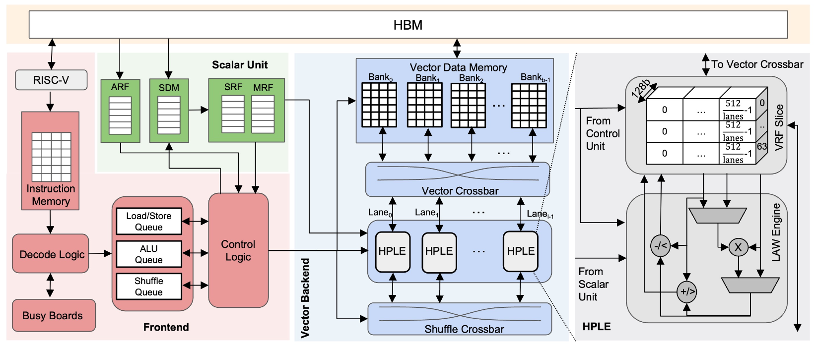
To tackle these challenges, a new approach is introduced: the Ring Processing Unit (Figure 1) and the B512 vector ISA. The B512 ISA is designed to cater to ring processing needs while remaining programmable for evolving algorithms and supporting post-fabrication software enhancements. The RPU, a highly parallel implementation of B512, features independent pipelines for data access, compute, and shuffle, along with a simple in-order front-end. A novel technique called busyboarding is introduced to manage register data dependencies efficiently.
To facilitate high-performance programming for RPUs, a new SPIRAL backend is developed. This backend leverages optimization techniques to compile and optimize code effectively for the RPU, particularly for complex operations like the NTT.
The RPU’s performance is evaluated using a detailed cycle-level simulator, considering various design parameters such as modular multiplier design, the number of HPLEs, and VDM partitioning. The optimal design point is validated through RTL implementation and emulation, with additional experiments conducted to assess the impact of optimized SPIRAL programs, multiplier design, speedup over CPUs, and area analysis.
Results
Methodology
A detailed cycle-level performance and functional simulator has been created to analyze the RPU and explore its design space. This simulator, programmed in C++, accurately models all aspects of the design and effectively processes B512 codes generated by SPIRAL. It can be customized to assess various VDM banking strategies, HPLE allocations, pipeline depths, and component IP configurations. Each component, such as HPLE, VRF, VDM, and others, is synthesized using Synopsys’ Design Compiler (DC) with GF 12nm technology targeting a 2GHz frequency. Memory components are modeled using a commercial SRAM compiler, and logic units’ area and frequency metrics are obtained from DC. Memory power consumption data is sourced from datasheets, while other component power consumption is determined using Synopsys DC. The simulations are conducted on a 32-core 2.5GHz AMD EPYC 7502 processor.
To validate the functionality, test vectors from OpenFHE are used to verify B512 code execution on the RPU. All codes generated by SPIRAL undergo functional validation in the simulator, and their outputs match those of OpenFHE. Additionally, a complete RPU design is implemented in RTL, synthesized, and emulated on a Palladium system. Real inputs from OpenFHE are used in these emulations, executing SPIRAL B512 programs under full circuit emulation. The outputs from the emulation are confirmed to match those of OpenFHE. Simulation performance estimates closely align with actual results, with a match rate of 97%.
NTT Performance
The RPU’s performance using NTT, vital in RLWE schemes, is assessed. For configurations with minimum (4) and maximum (256) HPLEs, trends were analyzed. With four HPLEs, doubling VDM banks largely increases area but minimally improves runtime. Conversely, with 256 HPLEs, doubling VDM banks notably enhances runtime with a slight area increase.
In terms of performance per area (P/A) for various RPU setups running 64K NTT, increasing HPLEs up to 128 banks improves P/A. However, further increases lead to a decrease due to expanded vector crossbar area. Similarly, enhancing VDM banks up to 128 HPLEs boosts P/A, but beyond this, the large HPLE area outweighs the performance benefits. Exceeding 128 HPLEs becomes impractical as crossbar costs become dominant.
Area Breakdown
When the number of HPLEs is fixed and VDM banks increase, the VBAR area grows as more banks lead to parallel transfers between VDM banks and HPLEs. Until 64 VDM banks, the VBAR area remains small for 128 HPLEs, then it doubles. Increasing VDM banks moderately increases the overall RPU area by 10%-24%.
With VDM banks set at 128 and varying HPLEs, doubling HPLEs doubles the LAW Engine area, and the VRF area increases by 1.5\(\times\)-2\(\times\). As the VRF is divided among HPLEs, each slice has fewer registers as HPLEs increase. This leads to smaller VRF slices mapped using less efficient memory macros, increasing area consumption. The VBAR area remains small but doubles with doubled HPLEs. Likewise, the SBAR area triples with doubled HPLEs, but for 256 HPLEs, it is 5\(\times\) larger than for 128 HPLEs.
Energy Consumption
When executing a 64K NTT on an RPU with 128 HPLEs and 128 VDM banks, the total energy used is 49.18\(\mu\)J. The LAW Engine and VRF contribute 66.7% and 19.3% to the total energy, respectively, making up 86% combined. Despite being eight times larger in memory size, the VDM consumes only 10.5% of the energy due to its efficient memory macros and less frequent access compared to the VRF. Additionally, each 128-bit modular multiplier dissipates significant power at 104mW, highlighting the need for future research into low-power designs. The vector crossbar and shuffle crossbar consume 2.3% and 1.0% of the total energy, respectively. The average total power of the (128, 128) RPU is 7.44W.
Impact of Code Optimization
The comparison of runtime between two programs executing a 64K NTT is conducted: one naive and the other optimized with SPIRAL. The variation lies in the number of HPLEs while maintaining the number of banks at 128. The unoptimized program lacks knowledge of the RPU microarchitecture, whereas the optimized one schedules instructions for maximum parallelism. On average, the hardware-aware optimized program runs 1.8\(\times\) faster than its unoptimized counterpart. Efficient scheduling of code is achieved by the optimized program, taking into account the underlying microarchitecture of the RPU. For example, with 256 HPLEs, shuffle instructions in the unoptimized code wait for 3,840 clock cycles to release resources from the busyboard, while in the optimized code, they wait only 128 clock cycles. This enhancement is attributed to SPIRAL interleaving independent instructions, thereby reducing stalls compared to the unoptimized program.
RPU Sensitivity
This sensitivity analysis yields two crucial findings: Firstly, it aids in hardware component selection, suggesting the adoption of a smaller multiplier with Initiation Interval (II) = 2 for the LAW engine, which performs similarly to a larger multiplier with II = 1 but offers reduced runtime. Additionally, it indicates that increasing shuffle latency could be advantageous if it leads to area reduction. Secondly, the study informs code optimization strategies by highlighting a greater sensitivity to load/store latency over shuffle latency. Consequently, prioritizing load/store instruction scheduling can significantly enhance optimization efforts.

Performance Comparison
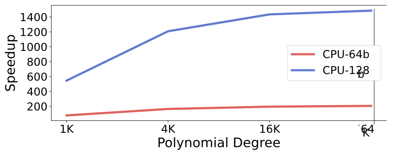
The study examined how the VDM interacts with HBM2 operating at 512GB/s. It assessed the runtime of NTT across polynomial degrees from 1K to 64K using the (128, 128) RPU setup. Comparing RPU performance with HBM2 against theoretical expectations shed light on load and store times and theoretical NTT execution latency. With increasing polynomial degrees, the RPU’s runtime neared the theoretical limit due to heightened parallel workload. The RPU demonstrated significant speedups over the CPU (Figure 2), ranging from 545\(\times\) to 1484\(\times\) for 128-bit NTT compared to the CPU. Even with 64-bit data on the CPU and a 128-bit RPU, substantial speedups ranging from 77\(\times\) to 205\(\times\) were noted. However, for polynomials exceeding 8k, doubling the degree led to a runtime increase of over 2\(\times\) due to data overflow, reducing the speedup over the CPU to 1484\(\times\) for 64K.
Critical Review
Pros
- It conducts a thorough analysis of the RPU, considering various configurations and factors such as hardware components, runtime, energy consumption, and performance sensitivity.
- The paper provides experimental validation through simulations and comparisons with theoretical models, enhancing the credibility of the findings.
Cons
- Lacks direct comparison with other HE compilers like Porcupine, Ramparts, nGraph, and Eva.
Takeaways
This paper introduces the RPU, developed to accelerate RLWE-based workloads. The RPU serves as an accelerator designed to support the proposed ISA, B512. Alongside the hardware, a compiler flow based on SPIRAL is presented to automate high-performance programming. Through the utilization of a newly developed simulator, the authors rigorously explore the design-space to understand tradeoffs and identify efficient designs. It is demonstrated that an RPU equipped with 128 banks and HPLEs can execute a 128-bit 64K NTT in 6.7 \(\mu\)s using 20.5mm\(^2\) of GF 12nm technology, achieving a notable speedup of 1485\(\times\) over a CPU.
References
- D. Soni, N. Neda, N. Zhang, B. Reynwar, H. Gamil, B. Heyman, M. Nabeel, A. A. Badawi, Y. Polyakov, K. Canida, M. Pedram, M. Maniatakos, D. B. Cousins, F. Franchetti, M. French, A. Schmidt, and B. Reagen, “Rpu: The ring processing unit,” 2023.
