Research Paper Review: Bridging the Computation Gap Between Programmable Processors and Hardwired Accelerators
The paper proposes a customized semi-programmable loop accelerator architecture that balances customization for efficiency with the flexibility to execute multiple similar loops. This accelerator outperforms a simple general-purpose processor in power efficiency by up to 34\(\times\) and in area efficiency by up to 30\(\times\). It only sacrifices as little as 2\(\times\) power and area efficiency compared to a non-programmable accelerator.
Paper Summary
The paper accurately predicts the increase in portable computer usage and the need for faster, energy-efficient systems with long battery life. These performance and energy demands are in direct conflict with the growing importance of post-programmability. While hardwired solutions excel in performance and power efficiency, programmable solutions offer unique benefits. Firstly, software implementations allow for the natural evolution of applications post-manufacture, accommodating specification changes, bug fixes, or new features. Secondly, multi-mode operation permits running diverse applications or variants on the same hardware. Thirdly, time-to-market for new devices is reduced through hardware reuse. Lastly, chip volumes increase as the same chip can serve multiple products within a family.
The core decision in hardware implementation revolves around balancing performance, power consumption, and programmability. Designers must weigh these factors carefully. This paper delves into a crucial question: How much programmability should a design possess? Traditionally, programmability is seen as a binary concept - a design is either programmable or not. However, it’s important to note that while programmable designs cater to a broad range of applications, hardwired designs are optimized for a specific algorithm.
The authors’ approach involves embedding programmability into a highly customized hardware setup to retain the high performance and energy efficiency typical of an ASIC while offering limited post-programmability. They start with a specialized loop accelerator (LA) designed for a specific application loop nest. Then, they expand the structure of this base LA template to create a semi-programmable solution called a programmable loop accelerator (PLA). The goal of programmability here is to map loops with similar computation structures onto a shared hardware platform. This could include two loops from the same application domain or a single loop that has undergone slight to moderate compositional changes.
The researchers examine the maximum performance attainable using various architectural styles, considering their programmability and power efficiency. They discovered that universally programmable solutions can accommodate any loop, albeit with differing efficiency levels. There exists a significant disparity between the efficiency of ASICs and these programmable solutions. The authors position PLAs in a design space where a significant level of programmability, along with the high-efficiency characteristic of ASICs, is necessary.
Moreover, they have analyzed loops in real-world applications and discovered that they undergo only minor changes over time. Generally, the core computation within the loop remains consistent, with small adjustments made to address bugs or introduce new features. Because these changes are not substantial, it’s feasible to design specialized hardware to speed up the original loop. This hardware can incorporate just enough programmability to effectively accelerate the loop as the source code evolves.
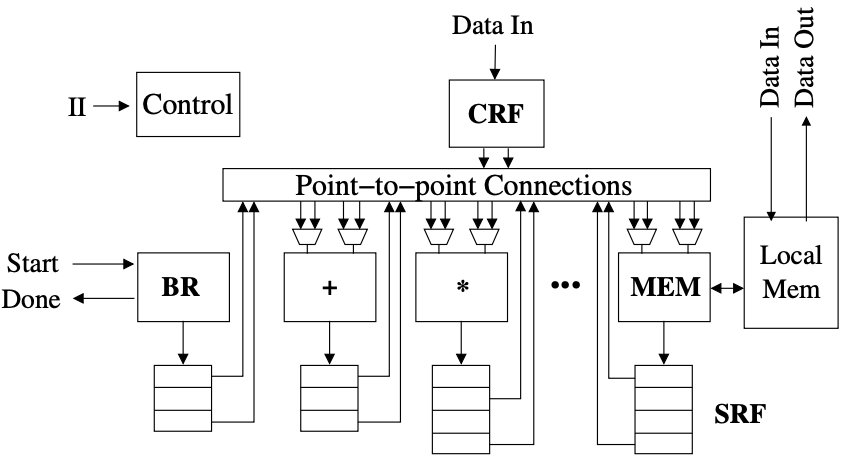
The paper establishes a single-function loop accelerator as a baseline. This loop accelerator (Figure 1) is crafted to efficiently execute modulo scheduling in hardware, a technique for overlapping loop iterations to enhance throughput. The LA leverages a high level of parallelism found in modulo-scheduled loops. Because an LA is tailored to a specific loop, its data path is customized to suit the computational and communication requirements of the loop’s scheduled operations. However, while this tailored data path ensures efficient performance, it also limits flexibility. When attempting to map a new loop onto an LA, even slight deviations from the original loop can lead to reduced performance or failure, primarily due to the restricted functionality and connectivity of the data path.
To create a PLA, the less flexible datapath features of the single-function LA need to be generalized efficiently in terms of power and area. The LA’s flexibility is constrained by the supported opcodes of the functional units (FUs). Generalizing FUs with additional functionalities that complement existing ones incurs minimal extra costs. These costs include increased hardware area and power usage, as well as encoding requirements for the expanded set of supported opcodes.
Two methods are employed to loosen the constraints of point-to-point connectivity. Firstly, all FUs gain the capability to execute a MOV operation, allowing the transfer of values between FUs via intermediate ones. Secondly, a low-bandwidth bus is introduced to connect all FUs, enabling a single value transfer from any FU to another each cycle. Although the global bus adds hardware costs, such as additional read ports in register files and new inputs in multiplexers, it enhances overall flexibility.
A broader strategy involves widening input multiplexers to allow each input port to access operands from any initially connected port. Using Rotating Register Files (RRFs) to replace Standard Register Files (SRFs) and enhance programmability, albeit at the cost of extra hardware for base registers, adders, and decoders. RRF sizes are rounded up to the next power of two to facilitate efficient register rotation implementation.
Introducing RRFs also impacts the control path, requiring addresses for each read and write port, unlike the address-less SRFs. To address this, staging predicates are broadcasted over a bus to all FUs, boosting scheduling flexibility with minimal additional costs.
For improved programmability, datapath control should be governed by signals from a control memory. Centralizing literals into a literal file allows the use of different literal values for different loops, enhancing versatility.
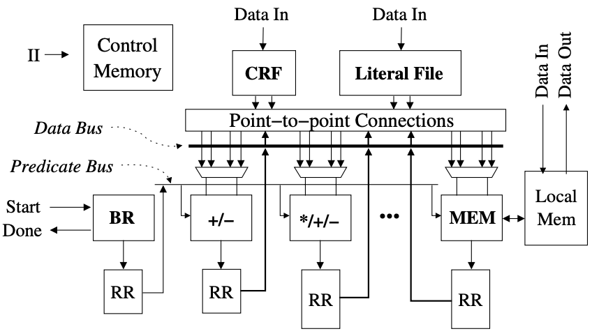
Figure 2 illustrates the template for the PLA, generalized from the datapath depicted in Figure 1. While the accelerator is tailored for a particular loop at a specific throughput, it features a more versatile datapath compared to the single-function LA, enabling various loops to be accommodated on the hardware. The FUs now support additional functionalities, a low-bandwidth bus links all FUs, staging predicates are broadcasted over a bus, SRFs are replaced with small, distributed RRFs; and the input multiplexers of the FUs are widened.
Results
The PLA architecture’s efficiency and programmability are tested using loop kernels from different application fields: signal processing (fir, fft, fmradio, bfform), media (dcac, dequant, fsed, sobel), and linear algebra (heat, lu). These loops vary in size, ranging from 17 to 60 operations. For each loop, Verilog code is generated for both single-function and programmable loop accelerators using the synthesis system. Synthesis and placement are conducted on the Verilog code using Synopsys Design Compiler and Physical Compiler, utilizing a 0.13\( \mu \)m standard cell library and targeting a frequency of 200 MHz. Power analysis is performed using PrimeTime PX after back-annotating the design with parasitics and switching activity information.
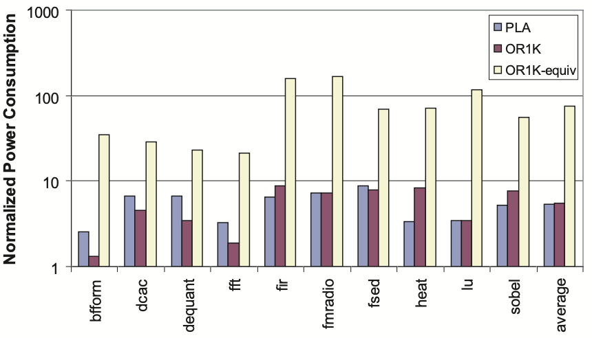
Figure 3 displays the relative power consumption of the single-function LA, the PLA, and the OR-1200 for each loop, shown on a logarithmic scale. It’s important to highlight that while the power consumption of the PLAs and the OR-1200 is similar, the PLAs perform significantly faster, ranging from 6 to 33 times faster than the processor. This difference in power efficiency is evident in the performance-equivalent bar. The graph indicates that PLAs consume about 2 to 9 times more power than their corresponding single-function LAs, which deliver the same performance. This increased power consumption is attributed to various factors, including the significant power consumed by the RRFs within the PLA datapath. Additionally, in the current setup, the RRFs are synthesized from behavioral descriptions rather than being generated by an RF generator, missing out on typical RF area and power optimizations like master latch sharing. Moreover, wider MUXes in the PLA contribute to additional power consumption. Finally, since the PLA datapath is more intricate than the single-function LA, when synthesizing both LAs with the same target clock frequency, the gates in the PLA will be sized larger to meet timing constraints, leading to higher power consumption. Comparing the PLA with the OR-1200 at the same performance level, the OR-1200 consumes 4 to 34 times more power.
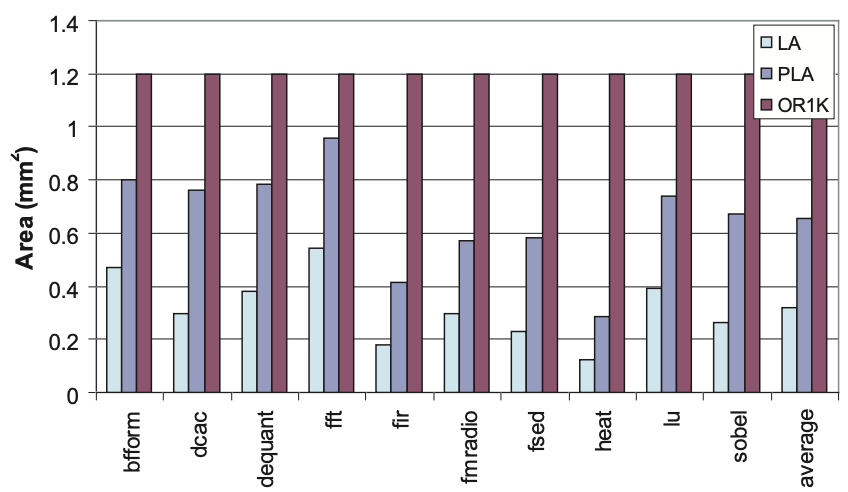
Figure 4 illustrates a comparison of the sizes of the single-function LA, PLA, and OR-1200. The PLA’s generalized datapath results in approximately twice the area compared to the single-function LA. In terms of area efficiency (performance per unit area), the PLA is approximately 30 times more efficient than the OR-1200 on average across these loops.
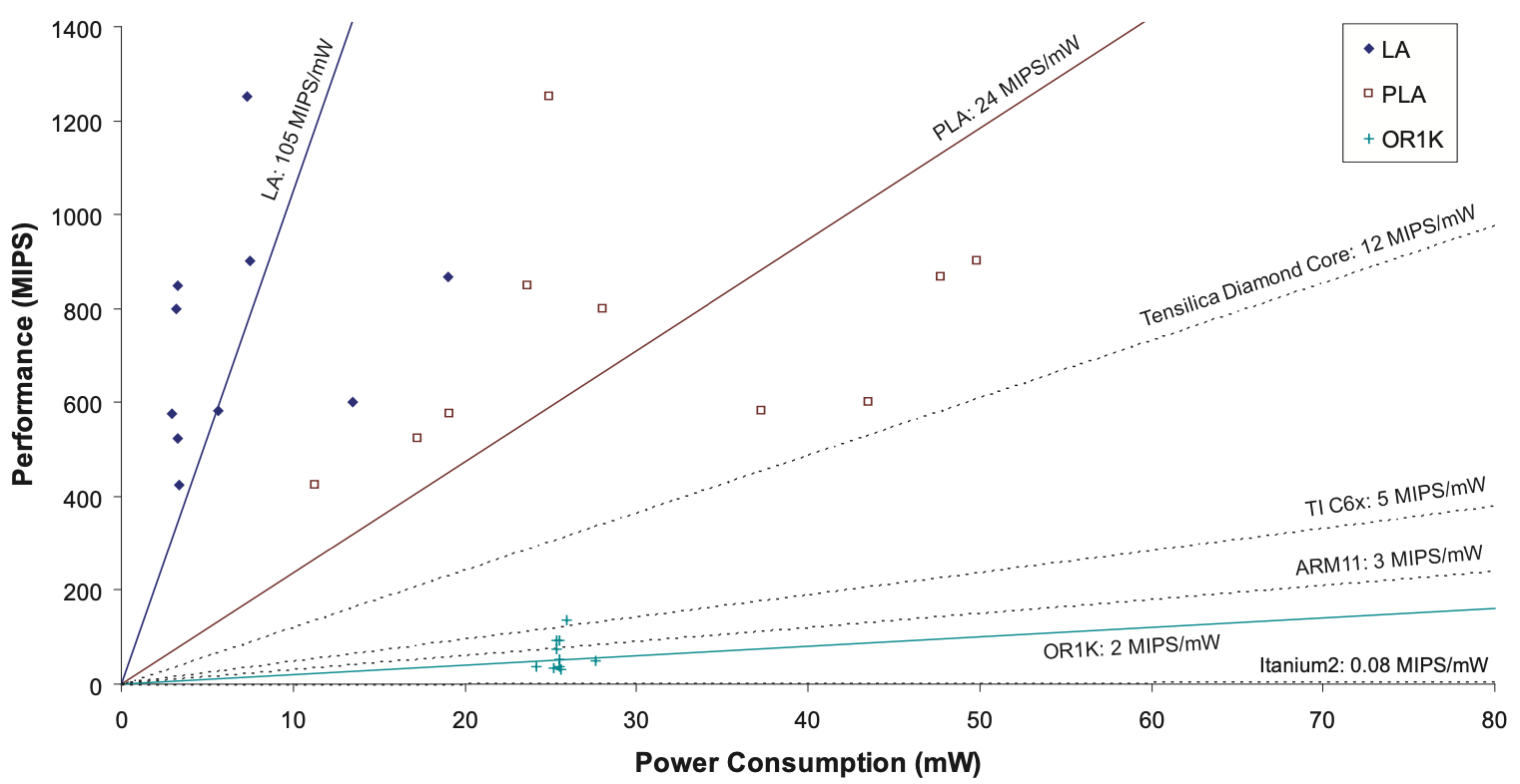
Figure 5 displays the relationship between performance and power consumption of the LAs and OR-1200. Points on the same slope represent roughly equivalent power efficiency, with points towards the upper left indicating greater power efficiency. Each type of hardware is represented by an average efficiency line. Across the designs analyzed, single-function LAs achieve an average efficiency of 105 MIPS/mW, PLAs achieve 24 MIPS/mW, and the OR-1200 achieves 2 MIPS/mW on average. The efficiency notably decreases as the hardware becomes more generalized and less tailored for embedded applications.
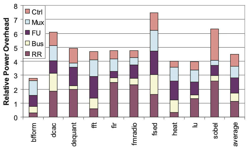
Figure 6 illustrates the power overheads associated with the main datapath generalizations in the PLA. Each loop is represented by a stacked bar indicating the proportion of power consumption attributed to different datapath elements. Typically, the RRFs and FU generalizations contribute the most significant overhead in the datapath.
The PLA is designed to operate semi-programmably, allowing it to efficiently execute loops resembling the one it was initially designed for. To evaluate its programmability, a loop perturbation method is utilized, introducing random changes incrementally to the original loop. Figure 7 illustrates, for each loop, the number of perturbations possible before the scheduler fails to map the loop onto the hardware without increasing the initiation interval (II). A higher number of perturbations indicates greater programmability.
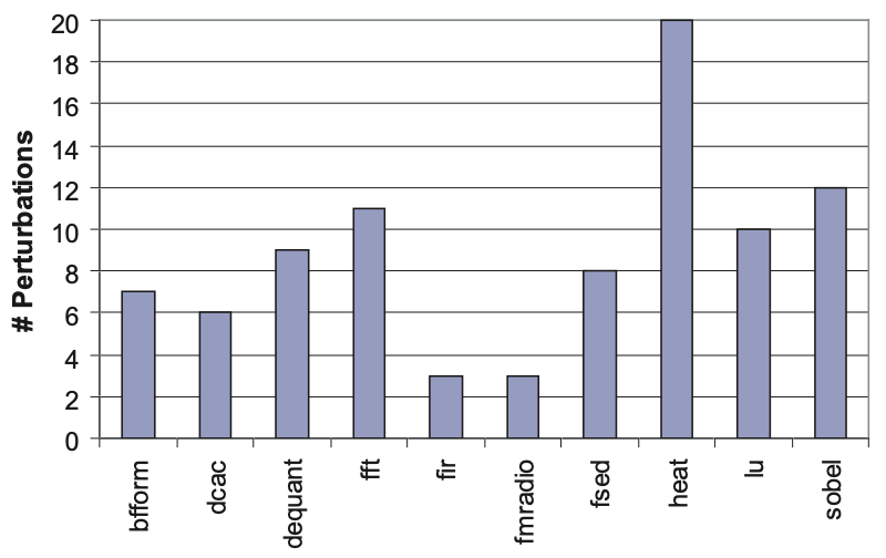
The graph demonstrates that the PLA’s programmability varies depending on the original loop. However, it solely depicts the number of perturbations feasible without performance loss. Generally, even after numerous perturbations, a loop can still be mapped onto the PLA if some performance loss is acceptable, facilitated by the global bus enabling data transfer between any FUs.
While the PLA efficiently handles similar loops, effectively executing arbitrary loops is improbable due to design tradeoffs. Nonetheless, in a cross-compilation experiment involving the 10 studied loops, mapping succeeded in 25 out of 90 opportunities.
Critical Review
Pros
- The authors correctly foresaw the popularity of portable devices such as cell phones, which have evolved to offer enhanced features and capabilities.
- The semi-programmable loop accelerator architecture achieves a good balance of performance, power consumption, and programmability.
- PLAs provide hardware reusability and significant enhancements in power and area efficiency compared to basic low-power general-purpose processors.
Cons
- Although the semi-programmable loop accelerator is effective for minor code alterations, it is not a fully general-purpose loop accelerator. Each accelerator still requires synthesis for a specific loop.
- The authors recognize a limitation: in a cross-compilation experiment with the 10 studied loops, only 25 out of 90 mapping attempts were successful, emphasizing a significant drawback of the PLA.
Takeaways
Customized loop accelerators offer significant gains in performance and power efficiency compared to general-purpose processors. By constructing semi-programmable accelerators, these efficiency gains can be maintained while allowing for hardware reuse as software evolves. The loop accelerator’s datapath is generalized efficiently, enabling similar loops to be mapped onto the accelerator. Programmable loop accelerators offer hardware reusability alongside substantial improvements in power and area efficiency compared to basic low-power general-purpose processors. In the loops analyzed in this paper, the PLA achieved 4\(\times\) to 34\(\times\) better power efficiency and approximately 30\(\times\) better area efficiency than a general-purpose processor, while trading off 2\(\times\) to 9\(\times\) in power and 2\(\times\) in area compared to a custom non-programmable LA.
References
- K. Fan, M. Kudlur, G. Dasika, and S. Mahlke, “Bridging the computation gap between programmable processors and hardwired accelerators,” in 2009 IEEE 15th International Symposium on High Performance Computer Architecture, 2009, pp. 313–322.
