Research Paper Review: A “New Ara” for Vector Computing: An Open Source Highly Efficient RISC-V V1.0 Vector Processor Design
The RISC-V V extension has recently reached the 1.0-Frozen Status. This paper introduces the initial open-source implementation, explores its influence on lane-based micro-architecture design, and offers insights into the performance-oriented design of coupled scalar-vector processors.
Paper Summary
The dominance of proprietary ISAs in top-performing super-computers hampers open innovation. In recent years, RISC-V has emerged as a well-established and openly available alternative to proprietary ISAs. Motivated by this, the authors directed their attention to the RISC-V Vector Extension (RVV). They present the initial open-source implementation, encompassing both hardware and software aspects of the RVV 1.0 ISA in this paper.
The Evolution of RISC-V V
The RISC-V V extension enables the processing of multiple data using a single instruction, akin to the original Cray vector processor. The initial RVV extension, proposed in 2015, introduced a Vector Register File (VRF) with 32 registers, each storing data elements of the same type. Vector operations typically work element-wise on two vectors, and support predicated computation allowing selective processing based on a Boolean mask vector. The current specification is v1.0, which is the frozen specification for public review. These are the notable modifications:
Vector Register File
The VRF is a critical component in vector processor design as it stores vector elements and heavily influences design decisions. In v0.5, the register file’s state was managed both globally and locally, allowing users to dynamically specify the number of enabled registers, with the hardware calculating the maximum vector length based on byte space distribution. Each register could be programmed individually to store different data types. However, in v1.0, the register file’s state is solely global. It consists of 32 VLENbit vector registers, where VLEN is a parameter indicating the number of bits in a single vector register. The parameter LMUL can be adjusted to change the register file’s granularity, for instance, setting LMUL to 2 results in 16 2 × VLENbit vector registers. Furthermore, the register file does not specify the data type of stored elements, leading to a more flexible architecture. Secondly, in v1.0, the striping distance (SLEN) parameter is equal to VLEN, making the VRF seen as a contiguous entity, and consecutive element bytes are stored in consecutive VRF bytes thus making it more lanes-friendly.
Instruction Encoding
In the earlier version, the instructions could use polymorphic encoding, as the data type of the vector elements was specified in a control register for each vector register. However, in the current specification, the encoding is monomorphic, and there are different instructions for different data types, therefore resulting in more instructions in the ISA.
Mask Register Layout
In v0.5, only one vector register could host the mask vector, and each element of this vector could host one mask bit in its LSB. This was updated in v1.0, where every register of the VRF can be a mask register, and the mask bits are sequentially packed one bit after each other, starting from the LSB of the VRF, thus adding more flexibility for the programmer.
RISC-V V and Lanes
The new architecture (VU1.0) is a flexible design with parametric VLEN aiming to achieve high performance and efficiency across various vector lengths. The paper highlights the importance of longer vectors to minimize strip mining. Strip-mining adds extra code overhead, which leads to increased bandwidth demands on the instruction memory and greater energy consumption during instruction decoding and processing.
VRF and Lanes
The VRF is implemented by splitting it into chunks, one per lane. This method allows easier scaling of the vector processors, as compared to a monolithic VRF. Furthermore, splitting the VRF offers more flexibility on the macro placement during the floor-planning of the vector unit and improves routing efficiency because the connections are local to each lane.
Byte Layout
In vector memory operations, the vector processor moves bytes from memory into its VRF. According to RVV 1.0, both memory and VRF layouts must match. This becomes problematic with a split VRF because subsequent elements should be placed in consecutive lanes to maximize Data Level Parallelism (DLP) and simplify mixed-width operations. Since element width can vary and the mapping between elements and lanes remains constant, the mapping between bytes and lanes changes. Consequently, the processor needs to track the element width of each vector register to restore its content, and any unit accessing a full vector register must be able to reorganize its elements.
Shuffle/Deshuffle
To rearrange data in the VRF, shuffling (bytes to VRF) and deshuffling (bytes from VRF) circuits are employed. This involves a set of byte multiplexers, one for each output byte.
RVV 1.0 Implementation Challenges
The changes introduced in RVV 1.0 simplify the interface to software programmers but add complexity to the design of a vector machine partitioned into lanes.
With RVV 1.0, every vector register can function as a mask register, and a lane can need mask bits stored in a different lane. Since data is shuffled within the VRF, we need a Mask Unit to fetch and rearrange the data, ensuring the masks are correctly applied to each lane. Introducing this unit increases routing complexity, especially when scaling to more lanes.
Furthermore, when the VRF byte layout is constrained (SLEN=VLEN) in architectures with lanes, specific instruction patterns can cause issues. The architecture should also support the tail-undisturbed policy, i.e. elements past the last active one shouldn’t be changed. To avoid corrupting these elements, VU1.0 must rearrange the destination register using the old and new Effective Element Width (EEW). This operation, called reshuffle, is done by the slide unit. The problem is worsened because programs can change the vector length and element width during runtime, making it hard to know how many bytes need reshuffling unless these are tracked dynamically for each vector register. Reshuffling affects Instructions Per Cycle (IPC), especially for narrowing instructions with the same source and destination registers, as it can’t preserve tail elements. Using tail-agnostic policies also has issues as leaving tail bytes unchanged can lead to corruption, while overwriting all with ones reduces IPC due to extra writes. Reshuffling is costly, particularly if the slide unit’s throughput is lower than the computational unit’s. Compilers and hardware design like a renaming stage can help mitigate these issues.
Architecture

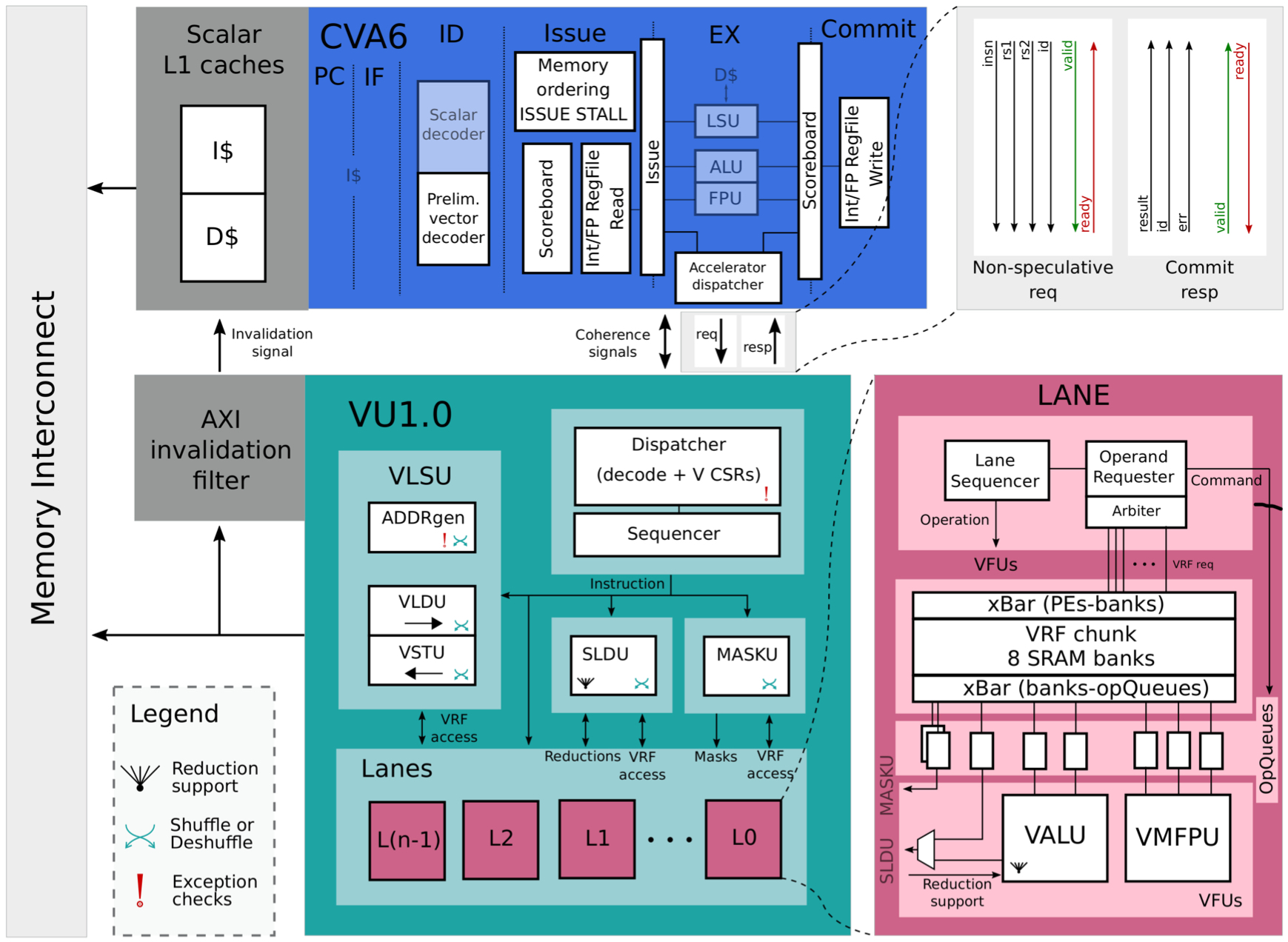
The unit supports the majority of RVV 1.0 with a few exceptions: no support for fixed-point arithmetic, floatingpoint reductions, very specific math instructions, segment memory operations, gather-compress, scalar moves, and some specific mask instructions. Figure 1 shows the main block diagram of the system.
In the updated architecture, since vector instructions specify the data types, it simplifies CVA6 unit and makes it agnostic on the V extension. All the decoding logic and vector-specific control and state registers (CSRs) move to the vector unit. CVA6 retains only the essential pre-decoding logic to determine if a vector instruction needs to be dispatched to the vector unit, whether it’s a memory operation (for cache coherency), and if it requires a scalar value from the integer or floatingpoint scalar register files.
The connection between the host processor CVA6 and the vector unit is simplified. The unit acts as a separate accelerator with its own control registers. During decoding, CVA6 recognizes vector instructions, adds them to a dispatcher queue, and sends them to the accelerator once they are confirmed to be non-speculative.
In VU1.0, a lightweight hardware mechanism is introduced to ensure memory coherence. The CVA6 data cache is modified to use a write-through policy, ensuring that main memory, accessed by both units, is always updated. When the vector unit performs a vector store, it invalidates corresponding cache lines in the CVA6 data cache. Additionally, scalar and vector memory accesses are regulated to prevent conflicts: scalar loads are issued only if no vector stores are ongoing, scalar stores are issued only if no vector loads or stores are ongoing, and vector loads or stores are issued only if no scalar stores are pending.
A Mask Unit is also added to fetch, unpack, and dispatch the correct mask bits to the corresponding lanes. The authors implement integer reductions using a 3-step algorithm: intra-lane, inter-lanes, and SIMD reduction steps. The intra-lane reduction maximized ALU utilization and efficiency by fully exploiting the data locality in each lane, reducing all existing elements. For inter-lanes reduction, data is moved and reduced among lanes in log2(l) + 1 steps, depending on the number of lanes l, using the slide unit. However, there’s a latency overhead due to communication between the slide and ALU units at each step. Finally, the SIMD reduction handles SIMD words, with latency logarithmically depending on the element width.
Results
The benchmarks used in [2] (fmatmul, fconv2d with 7 × 7 × 3 kernel) are manually optimized and adapted to the new specification and architecture, and compiled using LLVM 13.0.0.
To further understand the system, the authors conduct experiments to gauge how much the scalar core limits performance due to its non-ideal issue rate of vector instructions to the vector unit, showing how the scalar memory accesses impact the final throughput.

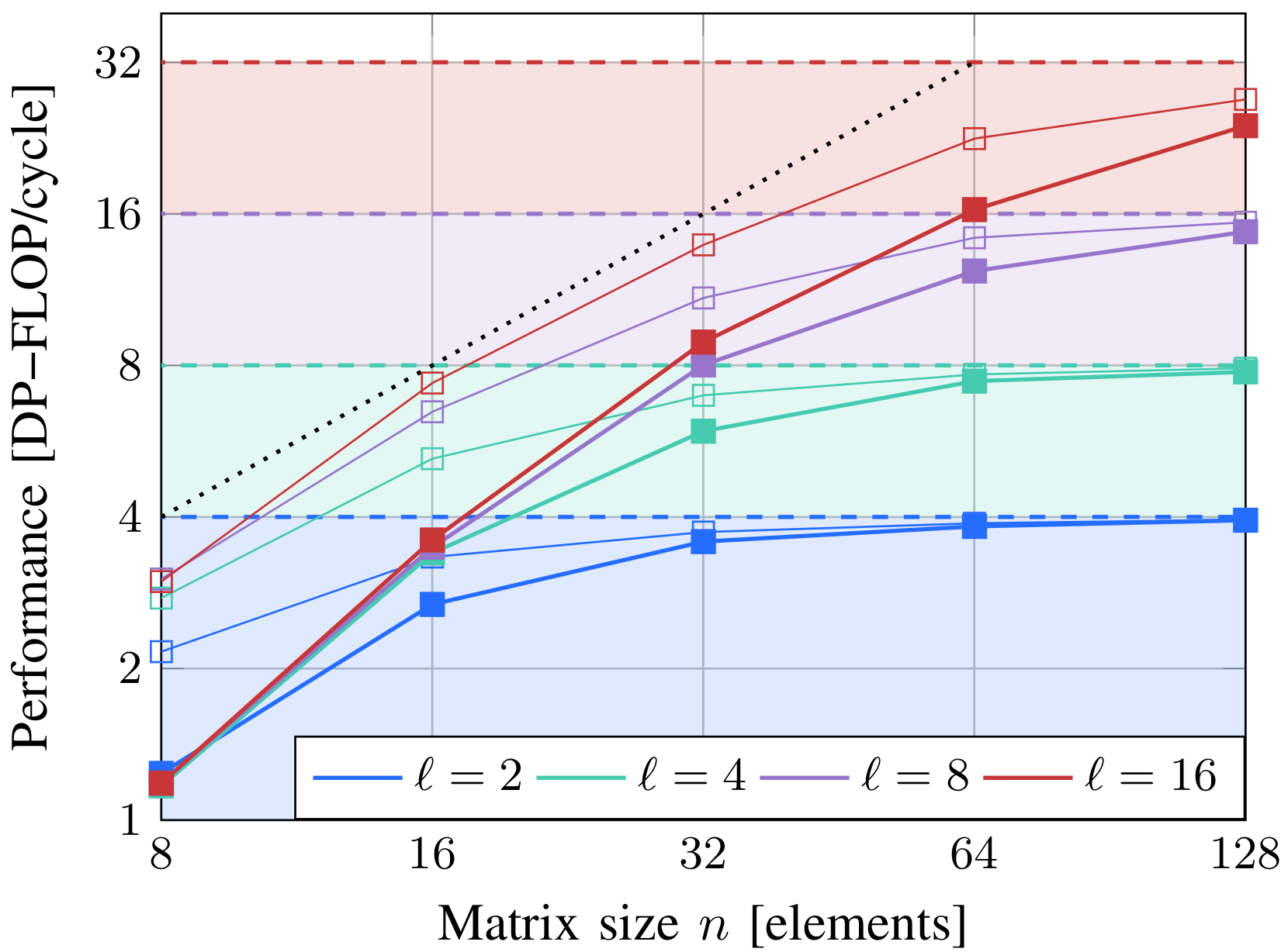
Figure 2 shows Ara’s roofline model for a variable number of lanes, and the performance results of the matrix multiplication benchmark between square matrices n × n for several matrix sizes n. The arithmetic intensity for this benchmark is proportional to n. The horizontal dashed lines mark the computational limit of the architecture for the corresponding number of lanes.
Even though the new architecture has VRF 1/4 of the size of [2], it achieves comparable or better performance for long vectors for both benchmarks, with a peak utilization of >98.5% with 2 lanes on 128×128 fmatmul. The utilization is almost 100%, hence, increasing the VRF size would barely increase performance for larger problems.
Figure 2 also depicts the performance of the real system alongside that of an ideal dispatcher. The ideal dispatcher’s simulation reveals the real performance limitations of the vector architecture and sets a hard limit on achievable performance, emphasizing the need to optimize the scalar part of the system.
In [2], a hard limit to the matrix multiplication performance was identified, especially for short vectors. With RVV v0.5 and their algorithm, the issue rate of computational instructions for the main kernel was one instruction every five cycles. However, with the new specifications, this has improved to one instruction every four cycles.

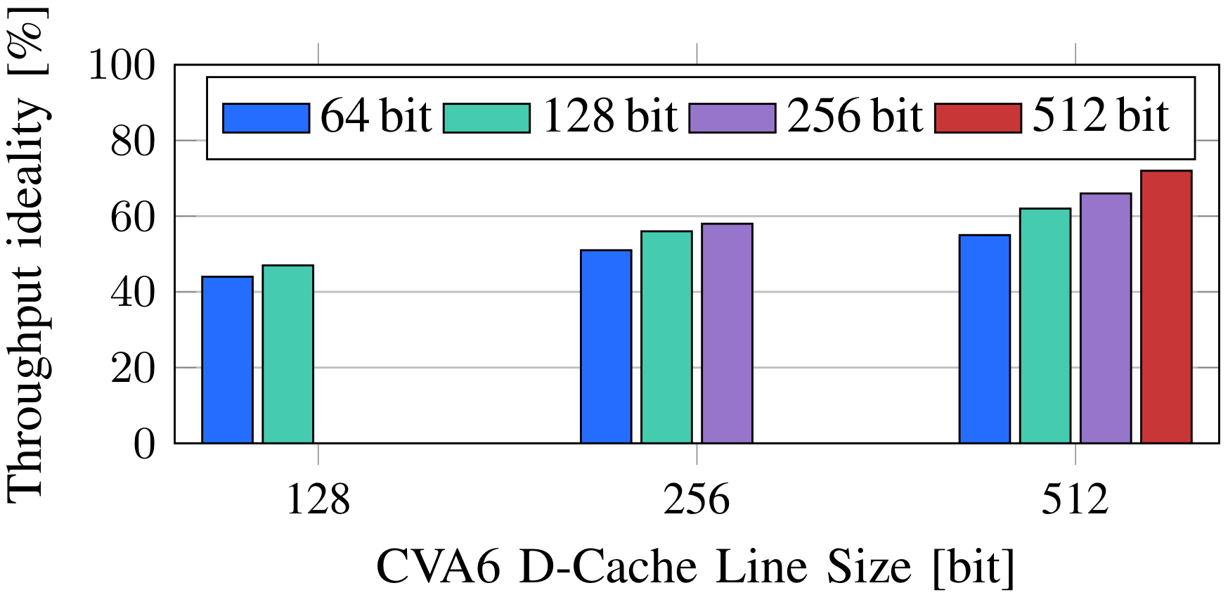
To assess the impact of the scalar part on performance, they modify the Advanced eXtensible Interface (AXI) data width of the memory port of CVA6 and the D-cache line width. This influences the miss-penalty and miss-rate of the scalar data memory requests, affecting the issue rate of vector instructions. Figure 3 summarizes the throughput ideality of a 16-lane system executing fmatmul on a 16 × 16 matrix while varying the memory parameters of the scalar core. Increasing the cache line size decreases the miss rate, but if done without widening the AXI data width, it negatively impacts the miss penalty. A wider AXI data width coupled with a larger cache line size significantly boosts system throughput, underscoring the importance of optimizing the scalar memory part for better performance on medium/short vectors.
Although the new specification improves the issue-rate limit for short vectors, their performance is still suboptimal. The VRF lacks the barber-pole layout, reducing effective banks in each lane and causing more bank conflicts. However, since the current architecture primarily focuses on long vectors, this isn’t a critical concern. Additionally, architectures like Hwacha and Ara faced similar challenges with short vectors despite implementing the barber-pole layout. Designers can address this by choosing a lower vector length or opting for more efficient non-vector SIMD architectures.
The authors also report that longer vectors prolong intralane reduction time, effectively concealing additional overheads and enhancing efficiency. While an increase in lanes accelerates intra-lane reduction, it detrimentally impacts interlanes reduction time in a logarithmic manner. Decreasing element widths enhances throughput with negligible overhead during SIMD reduction. Nonetheless, short vectors experience a startup delay, leading to decreased overall efficiency. For example, it takes approximately ten cycles for the vector unit to produce results after vector multiplication.
Furthermore, the study evaluates the impact of architectural changes on system performance, power, and area metrics by implementing a 4-lane enhanced design targetting GLOBALFOUNDRIES 22FDX FD-SOI technology. They synthesize and place-and-route the design, including CVA6, its caches, and the new vector unit, with VLEN = 4096 (16 KiB of VRF). The design is synthesized using Synopsys DC Compiler 2021.06 and physically implemented using Synopsys IC Compiler II 2021.06. Post-layout area, frequency, and power results are extracted through activity-based power simulations.
The design achieves a frequency of 920 MHz under worstcase conditions and 1.34 GHz under typical conditions, 7.2% faster than what is reported in [2] for V0.5, resulting in a 6.1% higher peak throughput in fmatmul compared to VU0.5. Despite a 4× smaller VRF compared to VU0.5, VU1.0 achieves an overall area reduction of over 15% without compromising performance. The energy efficiency of VU1.0 during a 128 × 128 fmatmul is 37.1 DPGFLOPS/W, only 1.9% lower than VU0.5, while supporting a more comprehensive ISA.

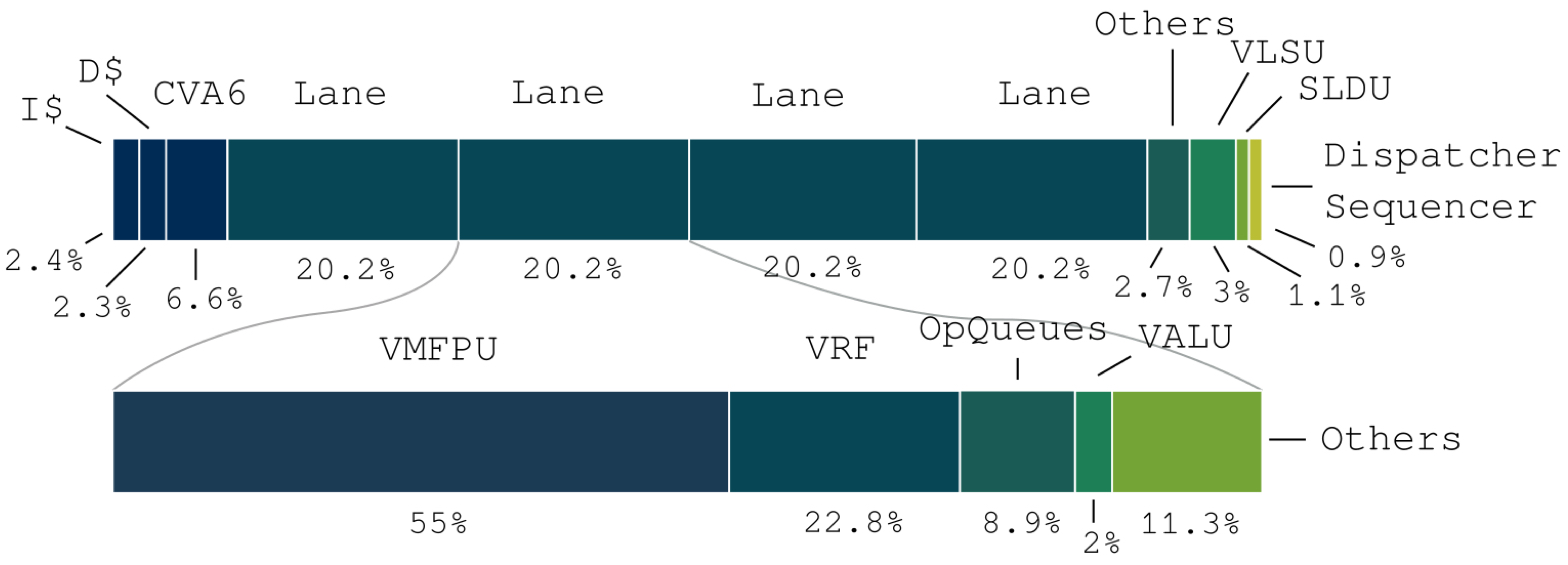
The power traces, Figure 4, of the system during a fmatmul run demonstrate how the vector architecture can handle stalls on the scalar core, maintaining peak utilization. The power breakdown reveals that more than 80% of the power is consumed by the lanes, with the VMFPU utilizing most of the energy, emphasizing the efficiency of VU1.0 in exploiting the regular execution pattern of vector machines.
Critical Review
Pros
- The paper introduces architectural modifications that simplify the interface to software programmers, at the expense of the complex design of a vector machine partitioned into lanes, and achieve competitive throughput compared to previous versions (VU0.5)
- Despite having a VRF four times smaller than VU0.5, VU1.0 achieves competitive throughput. This results in an overall area reduction of over 15% on the die size without compromising performance.
- While running a 128 × 128 fmatmul, VU1.0 consumes 280 mW, resulting in an energy efficiency of 37.1 DPGFLOPS/W. This is just 1.9% lower than VU0.5, despite supporting a more comprehensive ISA that includes reductions and memory coherence support.
- The paper demonstrates how the vector architecture tolerates stalls on the scalar core, maintaining peak utilization during computation.
- The hierarchical synthesis and backend flow significantly reduce turnaround time, enhancing design efficiency.
- The design and ISA are open source.
Cons
- While the paper presents improvements over previous versions, a broader comparison with other architectures or implementations could provide additional context.
- Complex logic for mask units and reshulffling impacts performance
- The architecture currently doesn’t support fixed-point arithmetic, floating point reductions and very specific instructions (round towards odd, reciprocal, square root reciprocal), gather-compress, and some specific mask instructions (e.g. vfirst, viota)
Takeaways
- The introduction of VU1.0 showcases the benefits of architectural modifications in improving performance, area efficiency, and energy efficiency in vector processing.
- VU1.0 demonstrates efficient resource utilization, particularly in the context of vector processing, contributing to overall energy efficiency in computing systems.
References
- M. Perotti, M. Cavalcante, N. Wistoff, R. Andri, L. Cavigelli, and L. Benini, “A “new ara” for vector computing: An open source highly efficient risc-v v 1.0 vector processor design,” in 2022 IEEE 33rd International Conference on Application-specific Systems, Architectures and Processors (ASAP). Los Alamitos, CA, USA: IEEE Computer Society, jul 2022, pp. 43–51. [Online]. Available: https://doi.ieeecomputersociety.org/10.1109/ASAP54787.2022.00017
- M. Cavalcante, F. Schuiki, F. Zaruba, M. Schaffner, and L. Benini, “Ara: A 1-ghz+ scalable and energy-efficient risc-v vector processor with multiprecision floating-point support in 22-nm fd-soi,” IEEE Transactions on Very Large Scale Integration (VLSI) Systems, vol. 28, no. 2, p. 530–543, Feb. 2020. [Online]. Available: http://dx.doi.org/10. 1109/TVLSI.2019.2950087
